Ulysses Flight Computer: Difference between revisions
m typo |
|||
| Line 10: | Line 10: | ||
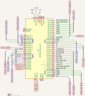
The Stamp has been chosen for the ease of mounting and for a lack of a commercially available RP2350 board / chip at the time of design. The main downside is the dimensions of the castellated board, which define the board layout. | The Stamp has been chosen for the ease of mounting and for a lack of a commercially available RP2350 board / chip at the time of design. The main downside is the dimensions of the castellated board, which define the board layout. | ||
The RP2350B is a dual core ARM-M33 '''or''' Hazard-3 RISV-V micro-controller with 520Kb of SRAM and 16 Mb of external FLASH memory. It has a flexible clock, varying from 150 MHz up to 200 MHz. | |||
It supports up to 2x SPI hardware channels, 2x I2C hardware channels 2x UART hardware channels and 4x ADC devices with 12 bits of resolution. It supports 48 GPIO pins with connection to 3 PIO blocks. | |||
==== programming the controller ==== | |||
The Stamp XL has 2 buttons marked "reset" and "boot". In order to program the board | |||
=== Power Supply === | === Power Supply === | ||
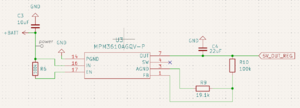
[[File:MPM3610 Implementation.png|alt=Implementation in the schematic of the MPM3610 Switching Regulatoor|thumb|Implementation in the schematic of the MPM3610 Switching Regulator]] | [[File:MPM3610 Implementation.png|alt=Implementation in the schematic of the MPM3610 Switching Regulatoor|thumb|Implementation in the schematic of the MPM3610 Switching Regulator]] | ||
The Ulysses flight computer uses an [https://cdn-learn.adafruit.com/assets/assets/000/127/631/original/MPM3610GQV-Z.pdf?1707519066 MPM3610] switching regulator with a maximum load of 1.2 A. This converts the +BATT voltage down to +5V. The voltage is then lowered by the Stamp internal LDO down to +3.3V. | The Ulysses flight computer uses an [https://cdn-learn.adafruit.com/assets/assets/000/127/631/original/MPM3610GQV-Z.pdf?1707519066 MPM3610] switching regulator with a maximum load of 1.2 A. This converts the +BATT voltage down to +5V. The voltage is then lowered by the Stamp internal LDO down to +3.3V. | ||
===== expected Power usage ===== | |||
=== Sensors === | === Sensors === | ||
| Line 26: | Line 35: | ||
=== I/O Ports & Connectors === | === I/O Ports & Connectors === | ||
===== Molex Nanoftis ===== | |||
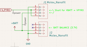
[[File:Ulysses Molex Nanofit.png|alt=Ulysses Molex Nanofit schematic for battery and pyro connections|thumb|Ulysses Molex Nanofit schematic for battery and pyro connections]] | |||
There are 3 Molex Nanofit connector, dedicated to the power management of the vechile and the connection to the Tracker: | |||
* The Battery connector with connections to the battery lead | |||
* The Pyro connector, which could be used to connect an external battery to use for the pyros or could be jumped to use the main battery. A specific connector should be made in order to jump the connector | |||
* The Telemetry connector which brings the battery cables to the Tracker along side a UART connection. The telemetry has the pins already switched in respect of the main board, so no null modem cable is required | |||
=== USB port === | |||
A USB type-c port is available on the side of the board. This may be blocked during assembly of the avionics bay. It is used for programming the board and recovering file in case of a filesystem in the FLASH memory. | |||
== History == | == History == | ||
Revision as of 08:46, 10 April 2025
Components
Controller

The board uses a RP2350 Stamp XL from solder party that, other than the micro-controller, mounts:
- 16 Mb of external FLASH
- 500 mA 3.3V LDO
- Footprints for external SWD and UART JST connectors
The Stamp has been chosen for the ease of mounting and for a lack of a commercially available RP2350 board / chip at the time of design. The main downside is the dimensions of the castellated board, which define the board layout.
The RP2350B is a dual core ARM-M33 or Hazard-3 RISV-V micro-controller with 520Kb of SRAM and 16 Mb of external FLASH memory. It has a flexible clock, varying from 150 MHz up to 200 MHz.
It supports up to 2x SPI hardware channels, 2x I2C hardware channels 2x UART hardware channels and 4x ADC devices with 12 bits of resolution. It supports 48 GPIO pins with connection to 3 PIO blocks.
programming the controller
The Stamp XL has 2 buttons marked "reset" and "boot". In order to program the board
Power Supply

The Ulysses flight computer uses an MPM3610 switching regulator with a maximum load of 1.2 A. This converts the +BATT voltage down to +5V. The voltage is then lowered by the Stamp internal LDO down to +3.3V.
expected Power usage
Sensors
lis3mdl
lso6dso32
bmp390
Pyro Channels
I/O Ports & Connectors
Molex Nanoftis

There are 3 Molex Nanofit connector, dedicated to the power management of the vechile and the connection to the Tracker:
- The Battery connector with connections to the battery lead
- The Pyro connector, which could be used to connect an external battery to use for the pyros or could be jumped to use the main battery. A specific connector should be made in order to jump the connector
- The Telemetry connector which brings the battery cables to the Tracker along side a UART connection. The telemetry has the pins already switched in respect of the main board, so no null modem cable is required
USB port
A USB type-c port is available on the side of the board. This may be blocked during assembly of the avionics bay. It is used for programming the board and recovering file in case of a filesystem in the FLASH memory.